Showing posts with label electronics. Show all posts

Wednesday, May 13, 2026

AI-assisted PCB design for energy monitoring (and scaling up don't trust the autorouter)

There is a specific smell to late-stage PCB work. A mix of coffee, solder mask anxiety, and the faint optimism that one more route pass will magically make analog behave. The poking around with oscilloscope probes and poring at datasheets to find out that you failed to pull reset low, out comes the magnet wires for a bodge.

Over the last week I have been building out an ADE9000 breakout with an AI-assisted workflow wrapped around KiCAD scripting. The results are useful, occasionally impressive, and still very far from “hands-off” for precision energy monitoring.

If you grew up with “don’t trust the autorouter” as muscle memory, good news: the saying still holds. We just scaled the blast radius from one menu click to an entire AI pipeline.
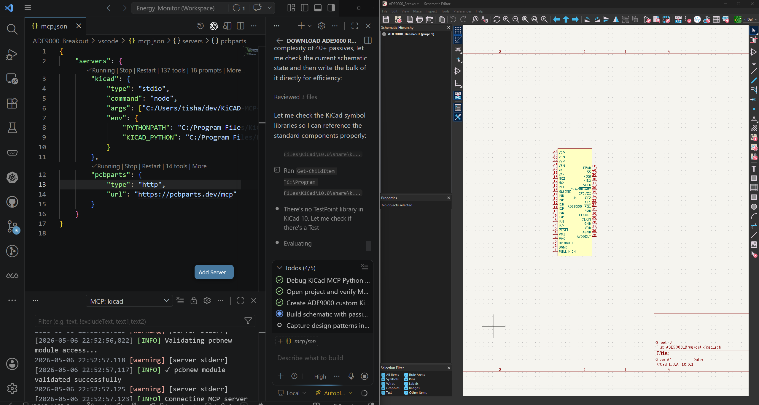
AI-aided KiCad schematic work in VS Code and KiCad

What changed on the board, not just on a slide deck

The recent commit sequence in ADE9000_Breakout tells the story better than any marketing copy:

  • d1e3352 (2026-05-07): “Initial AI Creation”
  • 043161c (2026-05-08): “Complete routing”
  • b8c8132 (2026-05-09): “Reroute with JST connector for SPI”
  • a469246 (2026-05-09): “Move decoupling closer”
  • 84b86e7 (2026-05-12): “Relayout using connectors for analog inputs”
  • 7d4b420 (2026-05-16): “Rerouted with Groundplanes and new skills”
  • c40e40a (2026-05-16): “Added License”
  • 9b2d97e (2026-05-17): “Add project-local 3D CAD assets”
  • cf8ba2c (2026-05-17): “Fix CT jack STEP orientation”
  • f5a11b2 (2026-05-17): “Remove CT jack pad overlays”

This was not a single-shot generation. It was iterative engineering with scripting and machine assistance in the loop:

  • Placement and connector mapping in scripts like place_pcb.py.
  • Deterministic route passes in route_pcb.py.
  • Critical route seeding and patching in seed_critical_routes.py and patch_remaining_routes.py.
  • Mechanical/silk cleanup with apply_board_markings.py and move_refs_to_silkscreen.py.
  • Continuous ERC/DRC artifacts (erc.json, drc.json) committed as hard checkpoints.
  • 3D STEP model handling pushed into the reusable layout and size-shape skills so mechanical review can keep pace with PCB edits.
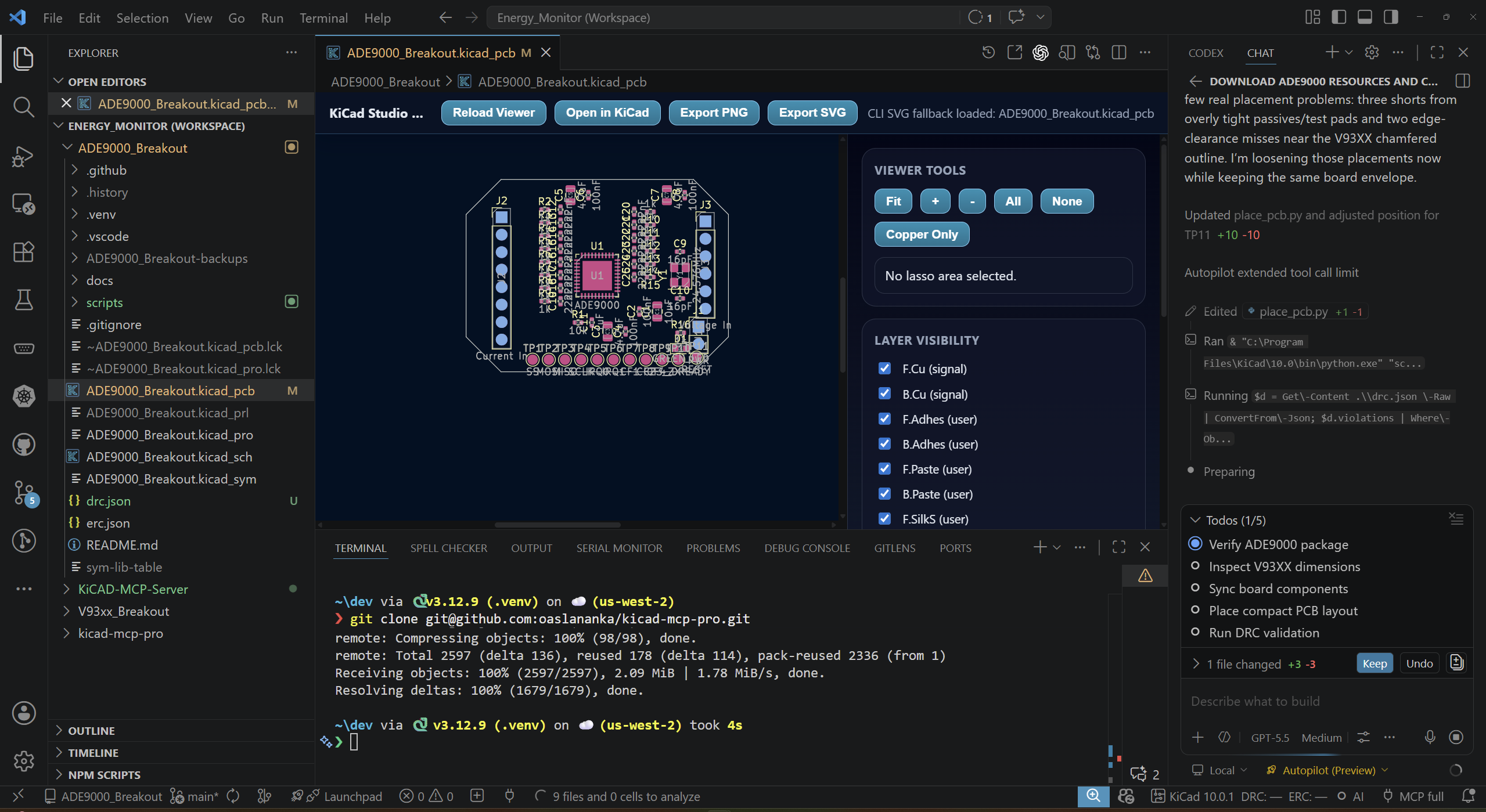
AI-aided ADE9000 PCB layout in KiCad

That pattern matters. The AI and automation stack gave speed and repeatability, but the engineering value came from repeated correction passes driven by board physics.

The same iteration loop is now visible in whatnick-energy-monitor-skills:

  • 335a718 (2026-05-16): Initial whatnick energy monitor skills
  • 78bfc44 (2026-05-17): Document STEP model workflow
  • 79d925d (2026-05-17): Clarify connector STEP model matching
  • af57c2d (2026-05-17): Document connector CAD alignment workflow
  • 32adeff (2026-05-17): Correct ADE9000 jack CAD guidance
  • d4167f6 (2026-05-17): Remove ADE9000 jack overlay guidance

That repo now captures reusable circuit, layout, routing, and board-shape guidance, plus the ADE9000 project overlay. The 3D model side was not a first-pass success either. STEP exports and connector models took multiple iterations before the project-local paths, model matching, and export workflow were stable enough to trust in a mechanical review. The later commits are the best evidence: first add local CAD assets, then discover the CT jack STEP orientation is wrong, then remove pad overlays that made the model look plausible while hiding the fact that the footprint and mechanical story needed to line up properly.

This is where AI-assisted hardware feels different from AI-assisted code. In software, a bad abstraction usually fails in tests or production logs. In PCB work, a bad abstraction can become a connector body floating neatly above the wrong pads in the 3D viewer. It looks professional right up until the part, enclosure, or cable says otherwise.
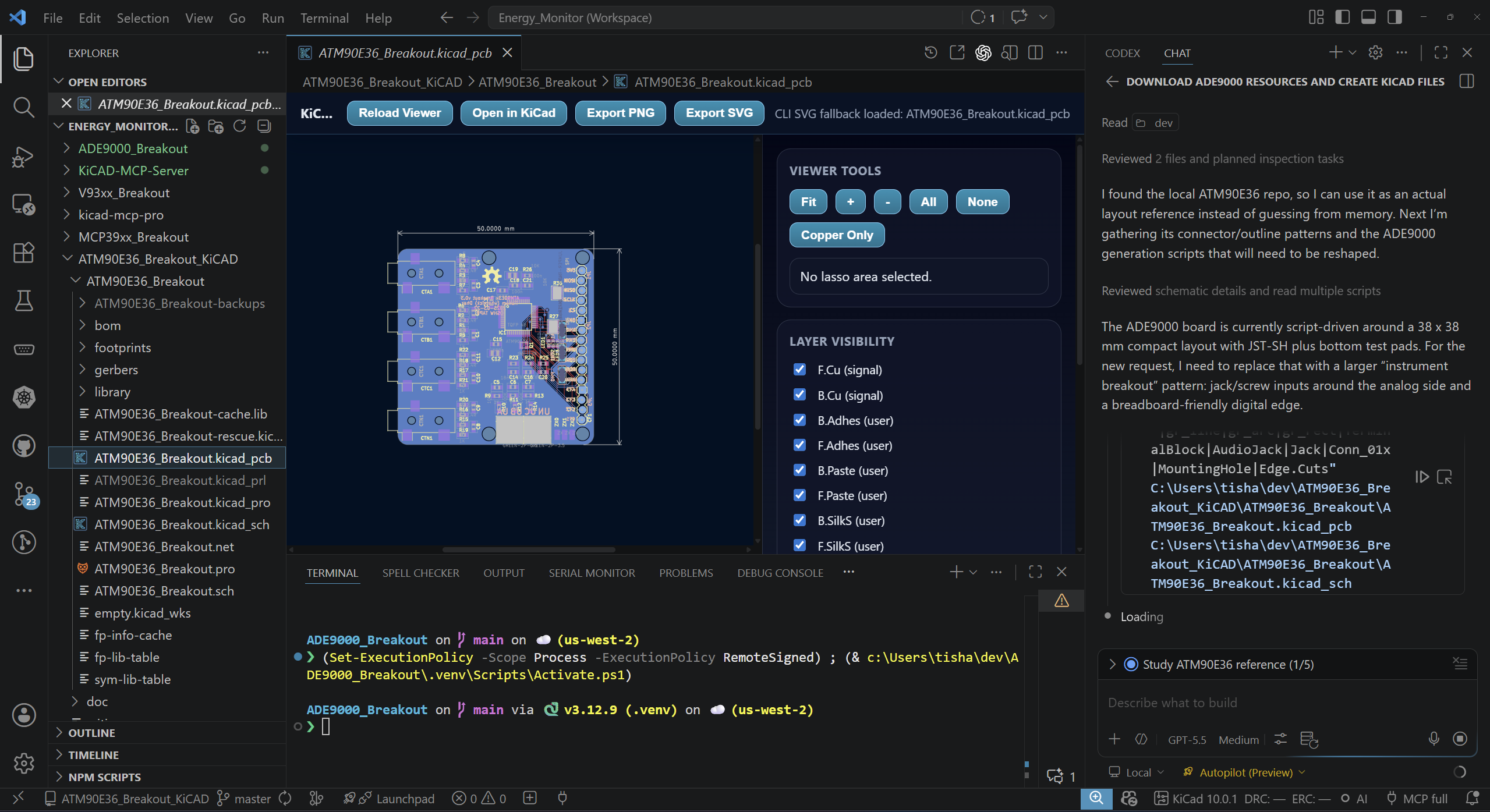
Pivoting the ADE9000 board toward the larger analog-connector layout

NotebookLM research: good at methodology, weaker on analog edge cases

I started on this adventure with posts from Samuel Beek promoting AI PCB design. I blended in my research background and curated a set of academic papers on AI/Algorithm usage in PCB place-n-route. I queried my pre-created NotebookLM notebook “PCB Place and Route Algorithms” specifically for mixed-signal energy-monitoring constraints.

The useful part of that synthesis:

  • Current AI placement/routing research still optimizes mostly for geometric proxies (wirelength, overlap, congestion).
  • Newer approaches improve constraint capture and collaboration, but are explicitly human-in-the-loop.
  • Model quality degrades on low-frequency pattern classes and novel interface combinations (cold-start behavior).

The important caveat from the same query was even more telling: source coverage was strong on AI placement methodology, but thinner on precision metering specifics like safety creepage strategy, return-current choreography around split references, and “what actually ruins ENOB on a real board at 2am”.

That gap is exactly the point.

Schematik, SnapMagic, and the new hardware workflow stack

Samuel Beek’s Schematik story is almost too perfect as an origin myth for this moment. An AI-generated wiring guide for a home-grown door opener took out the fuses in his apartment, which is a fairly direct way for physics to reject your prompt. Schematik has since raised $4.6 million from Lightspeed Venture Partners and is positioning itself as a “Cursor for Hardware”: describe a device in plain language, get a bill of materials, purchase links, and assembly instructions.

The interesting engineering choice is the safety boundary. Schematik is deliberately aiming at low-voltage circuits, typically 3-5 V IoT and maker projects, because that is where the promise is large and the downside can still be bounded. That is a sensible line. It is also a reminder that “AI for hardware” is not one market. The assistant that helps someone build an MP3 player is not the same system I would trust near mains metering, isolated sensing, or a DIN rail enclosure without a lot more constraint machinery around it.

SnapMagic is attacking a nearby but different layer of the stack. Its pitch is an AI copilot for electronics design, built on the huge CAD model base that started as SnapEDA: symbols, footprints, 3D models, part discovery, BOM optimization, supply-chain substitution, and integration with existing EDA tools including KiCad. That matters because a surprising amount of PCB time is not heroic analog insight; it is finding the right model, importing it cleanly, checking whether the footprint is sane, and making sure the thing still exists at Mouser or Digi-Key.

Schematik is closer to natural-language project generation. SnapMagic is closer to CAD-data and component-selection acceleration. My little ADE9000 workflow sits in the garage between them: NotebookLM for research synthesis, KiCad Python for deterministic changes, Freerouting for a first pass, project-local skills for repeatable domain knowledge, and human review for the parts that still smell like physics.

That is the practical opening for individual designers. You do not need to wait for one perfect vendor platform. You can build a small, opinionated workflow from pieces you already control:

  1. Put your design rules and recurring board-family choices into a local skill or checklist.
  2. Use AI for datasheet digestion, net naming, script generation, and alternative exploration.
  3. Keep KiCad, ERC, DRC, STEP export, and git history as the accountability layer.
  4. Treat external libraries like SnapMagic/SnapEDA as accelerators, then verify footprints, symbols, pin numbers, and 3D models against datasheets and mechanical reality.
  5. Let autorouters and AI propose routes, but hand-check return currents, decoupling loops, creepage, clocks, testability, and enclosure fit.

That sounds less magical than “hardware Cursor”, but it is much closer to how individual designers can safely get leverage today.

Why this hurts more on energy monitoring boards

An ADE9000-style board is not just “digital plus some analog”. It is a negotiated peace treaty between:

  • tiny differential analog signals,
  • noisy clocks and digital SPI edges,
  • shared ground structures,
  • high-voltage interfacing constraints,
  • and assembly realities.

AI can route what it can score. Physics punishes what you forgot to score.

For energy monitoring, the failure modes are often subtle first and expensive later:

  • A seemingly short route with a terrible return path becomes an EMI antenna.
  • “Close enough” decoupling in XY turns into high loop inductance in 3D.
  • Digital fanout convenience leaks noise into the measurement front end.
  • Clearance passes in one view while creepage silently fails along real surfaces.

The scaled-up autorouter adage

Classic autorouter distrust was about ugly traces and cleanup effort.

AI-assisted distrust is about false confidence.

You now get cleaner visuals, plausible routing, and confidence scores. The board can look more “engineered” while still violating analog intent. That is worse than obviously bad output, because it delays the moment when a human gets suspicious.

In the ADE9000_Breakout commits, that showed up as repeated topology and placement adjustments:

  • decoupling moved closer,
  • connector strategy revised,
  • critical nets explicitly seeded,
  • remaining logical gaps patched after freeroute import,
  • then relayout for analog input connector realism.
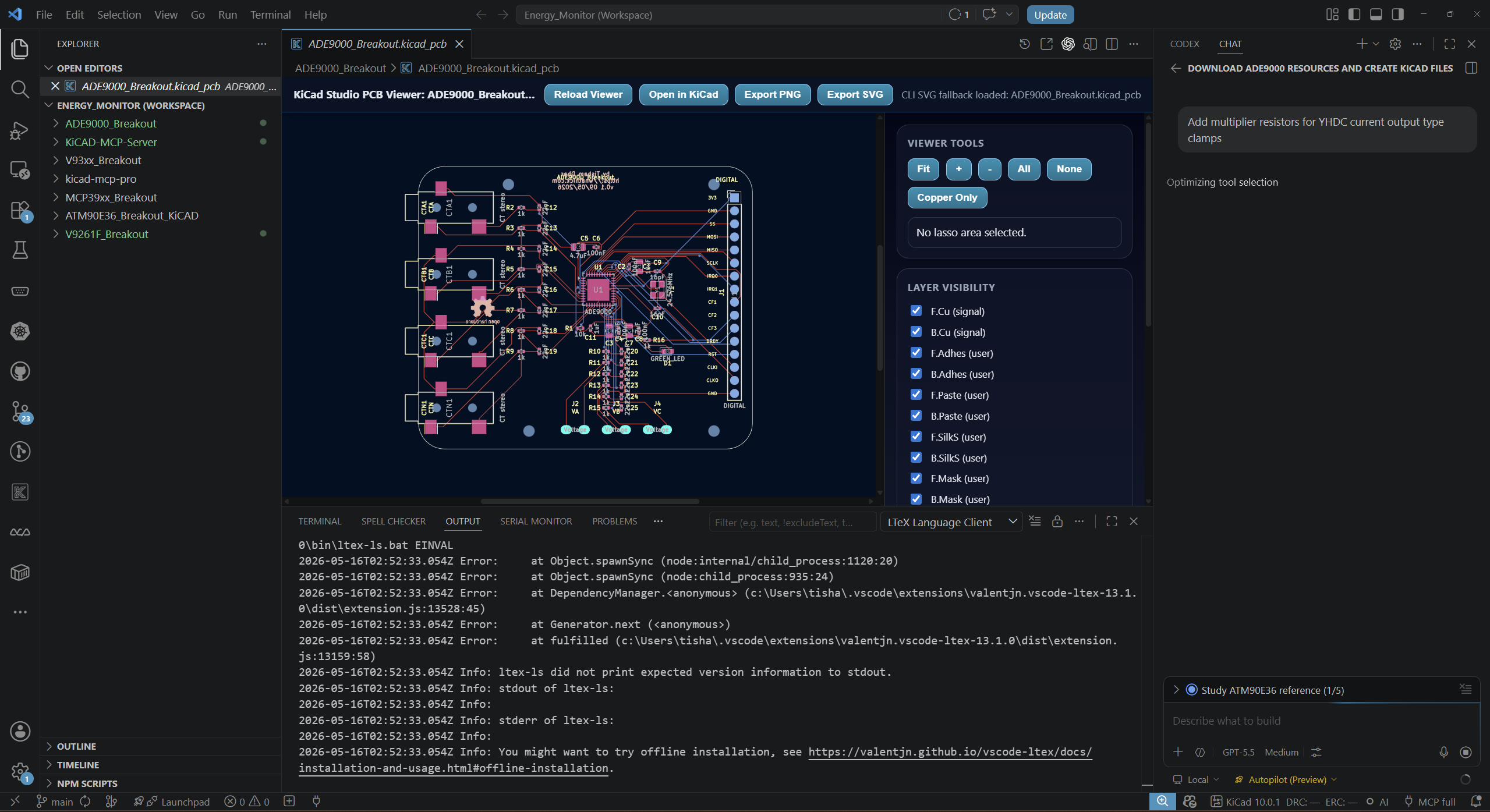
ADE9000 input clamp and analog connector pivot

None of that is anti-AI. It is pro-accountability.

A practical review checklist I now treat as mandatory

Before I trust an AI-assisted pass on a precision board, I manually review:

  1. Return current continuity under each critical signal path.
  2. Analog/digital ground interaction at the exact stitch points, not just net names.
  3. Decoupling loop geometry (pin, cap, via topology), not just nearest-component distance.
  4. Clock and fast digital net proximity to high-impedance analog channels.
  5. Creepage and clearance across real isolation boundaries and along surfaces.
  6. Testpoint access and assembly risks (reworkability, tombstoning, awkward probe points).

If any of those rely on “the model probably understood that”, I assume it did not.

What AI is genuinely good for in this workflow

After using it in anger, the wins are real:

  • Faster exploration of placement variants.
  • Deterministic scriptable edits to keep design intent reproducible.
  • Constraint management that catches obvious misses early.
  • Better ergonomics for repeated board evolutions.
  • Mechanical and export workflows, including STEP models, can be standardized, but they still need several passes to reconcile footprint libraries, connector variants, and CAD export paths.

This is similar to CNC in machining. You still need a machinist mindset. You just get to fail faster and with better logs.

The part that still needs engineers

The physics does not care whether a trace came from a human, an RL policy, or a nicely branded copilot.

Energy metering boards live or die on the details that are hardest to encode as generic reward functions. The edge where analog integrity, EMC, and safety overlap is still mostly tacit knowledge earned through measurements, bring-up scars, and post-mortems.

So yes, use AI aggressively for PCB work. I certainly am.

Just keep the old sign above the bench.

Don’t trust the autorouter.

Now it applies to systems, not just traces.

If you are building similar mixed-signal boards, I would love to compare review checklists and failure cases that escaped DRC but showed up on the bench.

Saturday, November 5, 2022

Drop shipping products from PCBWay

Drop shipping products from PCBWay

For a while I have been ordering PCB’s from PCBWay and parts from Mouser and Digikey, then hand assembling them at home. These have been very small scale cottage industry style runs and ultimately time consuming as I focus more on design and evaluation of new energy monitor ASIC’s such as the V9261F. When PCBWay started offering to stock and drop ship my PCB’s directly from the factory using their extensive clout with DHL, I promptly signed up for the service.

Recently I have been getting my ATM90E36 Devkit PCB’s assembled there. The service has been excellent with concierge like parts choice and purchase. Followed by extremely helpful consultation on assembly progress and correctness.

I received the following images after the first stage and confirmed the crystal and LED’s.


Then I received some more inspection photos to allay any doubts.


Looking forward to the stock appearing on the shop front.

NOTE: This is a paid promotion of PCBWay services

Thursday, May 7, 2020

ADE7816 Energy Monitor

I have been meaning to try out the ADE7816 Single-phase 6 current channels energy monitor for a while. However time has been lacking for the last couple of years. Finally I have a working version with successful board bring-up and a semi-working Micropython driver, with an Arduino driver in the works.

PCB Design

The PCB design process for this was not easy mostly due to a footprint choice mistake on my part. I had placed the 5x5mm QFN part instead of the 6x6mm QFN part in KiCAD. This made the DRC fail everywhere in standard settings. However it ended up being a collaboration opportunity with Greg Davill who loves to practice and photograph bodging stuff. So I now have a work of art at hand instead of a non-functional board.

I am even debating whether to place the rest of the parts and possibly take away from the dead-bug awesomeness. Next time need to order parts in advance and make sure I do 1-1 prints to verify footprints before pulling the trigger on PCB's.

Energy Montor Details

Now to more about the energy monitor. This ASIC features 3 single-ended and 3 differential current inputs and a single-phase voltage input, all in very compact 40-pin 6x6mm QFN package. In fact the PCB is large on purpose to accomodate ease of use with stereo-jack type current clamps. The main usage would be in standard households where there are typically 3-4 lighting circuits, 1-2 socket circuits and dedicated Air Conditioning circuit. A single energy monitor could be built to monitor all channels using a single-ASIC and leave out fancy NILM stuff from worrying about the lights. The socket circuits could have anything plugged into them and can potentially have point-of-load monitoring instead of breaker board based monitoring. All this translates to more data being generated for IoT platforms and some sensible firmware work needs to be done to handle that.

ADE7816 Driver Development

This is still work in progress. I have done some initial exploration to find prior art. Nothing exists yet from Arduino however there is some register lists from a Javascript driver written for the now defunct Intel Edison.

Intel never quite had the maker market pinned right to market that board, it makes me sad to think of all the engineering ours sunk into a now defunct platform. Open-source software / hardware helps us salvage some of that. I also sped up the register listing by copy-pasting the ubquitous table from the ADE7816 datasheet and dropping it into a Jupyter notebook to parse all the registers, not as fancy as the Pdf parser I had built before, but much more reliable.

My driver development follwed the now tried and tested Micropython + Jupyter Notebook + Logic Analyzer path. I used an ESP32 feather as host processor with standard micropython loaded and probed the SPI bus with read-write packets for known registers until the protocol gave in and started responding with some values. The ASIC is super versatile in supported protocols - I2C Slave, SPI Master and SPI Slave modes are all viable. So developing a fully functional driver supporting all the possible modes will take a while. The initial work so far is on the SPI slave mode since all my other work in DIN rail and Featherwing formats is linked to the SPI bus, however the I2C mode can be really interesting for host-processors with fewer pins and flaky SPI support (while having solid I2C support - like the Onion).

If anyone is interested in driver development I am happy to send you a board or you can get one yourself from Oshpark, Aisler or PCBWay. Once the drivers mature I will list it for a wider audience on Tindie.

Friday, January 24, 2020

Testing the OrangeCrab r0.1

After hassling Greg Davill for a while on twitter and admiring his OrangeCrab hardware I managed to catch up with him in person in Adelaide. I have been away in Nairobi till October last year, then I spent a brief few days in Adelaide before coming over to Canberra to take up a position in Geoscience Australia. The new gig is much less time commitment than the start-up world and hopefully will allow more time for blogging and board bring-ups like this one.

I caught up with Greg at a Japanese restaurant in Rundle mall and was treated to his now trademark led cube and led icosahedron. They are insanely detailed pieces of work and deserve staring at. However I am most grateful for the care package he left me, an OrangeCrab v0.1. This is an ECP5 board in feather form factor with an ADC built in to respect the Analog In pins on the feather. My aim for this board is to host some energy monitoring code on the FPGA with a fast 4mbps or so ADC and perform power/energy calculation on some parts of LUT's/DSP and have a softcpu push data out.
Greg also left me a home-made FTDI based board to use a JTAG programmer. The whole setup requires 3 USB cables:

  •  To plugin and power the FPGA board (eventually it should be alos programmable via this port) 
  • To attach a USB-Serial converter and watch the console when the gateware comes up 
  • To program the board over JTAG using an FTDI chip


Getting firmware compiled these days is getting easier, but Greg had done his initial testing with Lattice Diamond. I managed to installed it in WSL and promptly ran into a tonne of issues. The weirdest being close coupling to bash, Ubuntu actually uses dash as its default shell. You can get a Diamond licence and help support integration of diamond in litex-buildenv.
I was about to give up then Greg got it working with the opensource toolchain and [NextPNR-ECP5. I had by then setup litex-buildenv to support the orangecrab. So getting some gateware on was relatively easy. Then I got stuck on RAM timing bug in Litex till a few hours ago when I tested out some new gateware.

Also Checkout out Greg's foboot fork and help make programming over the USB possible and reduce 1 USB cable. More work on this including getting MicroWatt running coming soon.

Wednesday, June 26, 2019

Sunbeam Coffee Maker Teardown

The bad Kenyan grid has struck again. There is very little built in surge protection in the system, so all appliances plugged to the wall end up with in-house surge protectors. This time the victim was my beloved coffee machine which had served us well for more than a year.

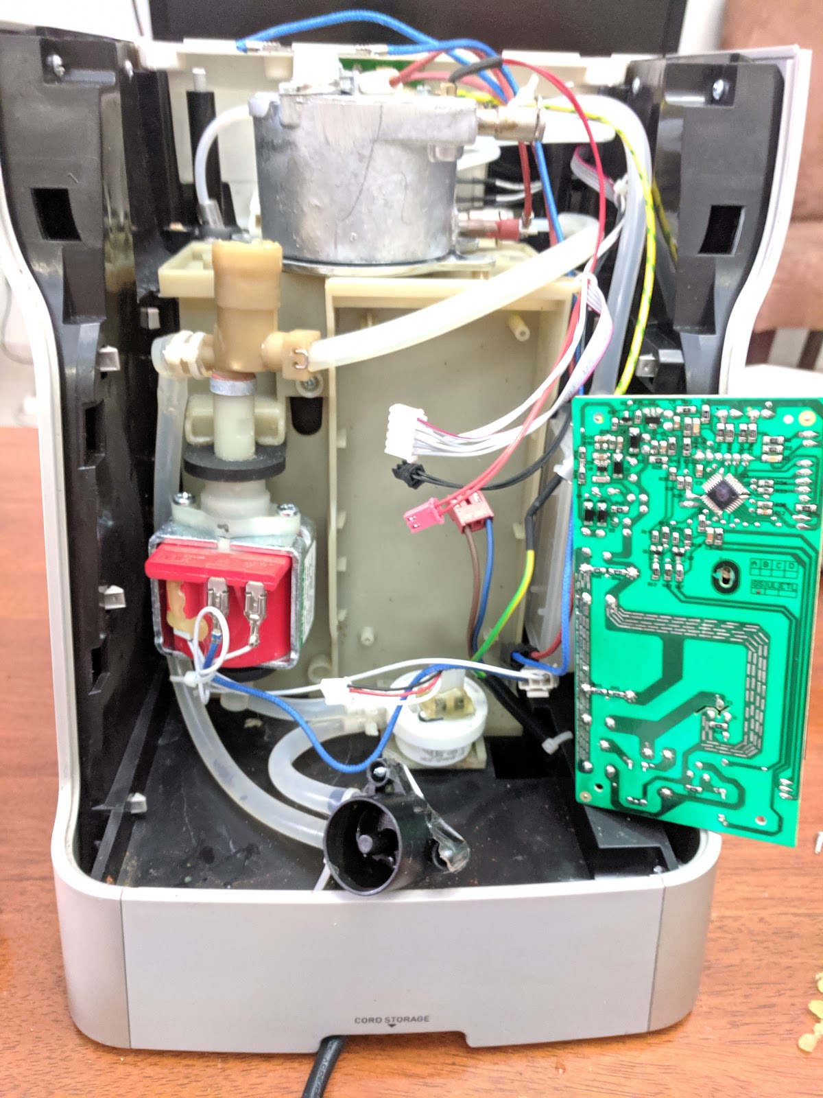
So I decided to take it home and spend some quality time with Pascal tearing it down. He is always curious about stuff and what is inside, so the Coffee machine is a complex beast capable of keeping him and myself occupied for hours on end. First we took of the top and looked at the heater and the electromechanical assembly controlling the hot-water head and frother was exposed. Also was exposed the heating tank with dual heating elements and a thermistor (I am assuming a thermistor rather than a thermocouple).

When we took the back plate off we found the main controller board. There is to obvious transformer in the set-up so I assume to whole power supply is cap-drop. There is a giant heat-sink attached to a 3-pin device which I assume is a triac or SCR for controlling the heating elements.

The bottom-left corner has a water pump with its own switching mechanism driven by relatively thin signal-wires from the main board.

There are some more interesting details on the main processor board including thick high current traces driven by the silicon switch with exposed copper and extra solder on top to increase thickness and provide a lower current path.

The main CPU is TQFP packaged micro-controller which is covered by the conformal coating the entire PCB is covered in. A macro image on twitter helped establish the lineage of the processor. It is a chinese 8051 variant with the datasheet here. Any help in translating it will be highly appreciated. But most of the schematic is legible.

Next up will be powering on the processor with a suitable 3.3v supply and examining the analog and digital buses. As well as powering on the whole thing to see why it turns of immediately on start. If the machine is unfixable I am planning to scavenge the thermistors, heating elements etc. to build a reflow mechanism.

All the water circulation mechanism is really interesting as well and can possibly be shoe-horned into a water cooler for a 3D printing system.

Saturday, June 22, 2019

Nairobi 2nd OSHW meetup

After a many month hiatus we finally put together the 2nd Nairobi Open-source hardware meetup. This time we were at the Tav Irish Pub near Nairobi Garage on Waiyaki way. The pub was chosen due to proximility to Nairobi garage and possible use of that venue. As it turned out none of us were memebers paying the $60 per-month fee so we ended up co-opting the pub in Chicago 3H fashion.
PCB Lineup
PCB Lineup
I had collected PCB's over the last few month from Aisler, OSHPark and PCBWay all shipped to Kenya from Germany, US and China respectively. So we lined up to try various soldering techniques on 0603 Jellybeans and some 20pin TSSOP IC's.
Soldering demo
Soldering Demo
The techniques we we tried were the tack, finish and reflow one using the iron and an experimental one with paste and dry-iron I had picked up recently. I didn't have a temperature profile controller for the dry-iron method. So we were just going to wing it by the eye.
Part Placement
Part Placement
We pasted up the boards using screwdrivers and tweezers. Started the reflow till the parts settled. Then simply turned off the iron. I am sourcing a K-Type thermocouple and SSR from KTechnics to get a better handle on this for next time. However the dry-iron does reach sufficient temperature for leaded solder reflow.
Dry iron reflow
Dry iron reflow
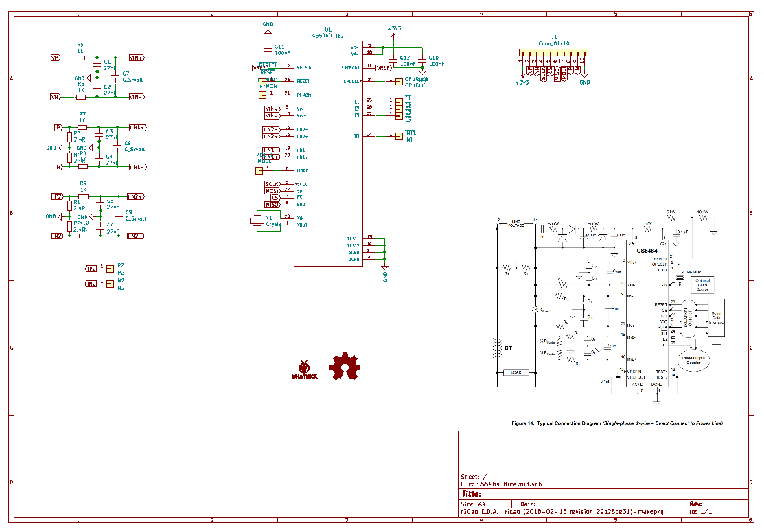
By the end of the session we had assembled x2 CS5464 Breakouts. Next step from here will be suitable MicroPython and Arduino drivers to ensure these things actually work. We had a lot of fun over the meetup and I hope to continue having these sessions. Next time one of the participants has promised to bring his Weighbridge Automation and IoT set-up.
Scavenging Coffee Machine
Scavenging a Coffee Machine
Following the meetup I have been hunting for accessories to make the dry-iron reflow less of a fire hazard and more controllable. (Un)fortunately the coffee machine at work has been fried by the spikes prevalent in the grid in Kenya (especially during the rainy season), so I have a spare K-type thermocouple I can work into the build. I have also co-opted a tissue holder we had on our dining table to stabilize the inverted iron during reflow.
A stand of opportunity
Stand of opportunity
Onwards to the next Meetup.

KiCon 2019 - Chicago in a weekend

Getting away from a fast paced start-up to attend conferences is a hard ask. However I managed to get away for a few days to attend the inaugural KiCad conference in Chicago a few weeks ago.
The pace has been such that only after about a month I am getting a chance to write it all up. The first night I managed to attend the Hardware Happy Hour at the Ballast Point. I got to see some amazing stuff including pneumatics for an autoplaying piano using layers of PCB.
The huge selection of beers and the chicago dogs were definitely unexpected bonuses.
Tour of MHub assembly area with pick and place machine and large Molex sign. Also got to see Chris Gammell's desk and pick up some Amazon and Mouser shopping to bring back to Nairobi.
I could definitely use the pick-n-place machine in my house and I hope Chris makes use of it whenever he can.
I also got to speak to some companies I have worked with remotely but not met the principles and representatives in person, including CrowdSupply, Aisler, SnapEDA, Hologram and of course DigiKey. It was great to speak to the KiCAD dev team as well, perhaps I can contribute on the MSVC windows native build. I also managed to score credits freebies from all the sources.
Here are pure notes to self on various topics that I picked up on 2-days of super varied and dense conferencing. Some are commands I would like to run some, are techniques I learnt and some are pure stories I picked up.

Schematics are a drug, use code instead

  • pip install skidl

Auto-routers are evil but useful

  • Triangles (Topological/ Using TIN mesh)
  • Maze solving
  • Shape based ( Rectangles)
  • Channel Based
  • FreeRouting
  • Adaptive heuristics using deep learning
  • Linear increase in PCB complexity

High-frequency simulation (in GhZ range) for PCB's

  • OpenEMS ( MEEP)
  • Wilkinson filter
  • Important in Radar Design

Prototyping in a few hours

  • Isolation milling
  • Midwest Circuit Technologies
  • Bantam tools. Binary save.
  • 1/32" end mill 0.8mm tool
  • 10 mill trace

Rendering photorealistic PCB's

  • Render layers to image texture
  • Use Blender cycles based render with bump maps for silk-screen and traces

Contributing to KiCAD

  • Development in LaunchPad + Github
  • Starter bugs are available

More HF PCB's

  • 30MHz to 3Ghz, with narrow bins
  • 5.6GSPS digitizer
  • Tuned lines. Right angles create problems.
  • Use footprint, Arc or Trace around edge cuts.
I woke up pretty early on Saturday morning and walked around and almost hopped on a fire-engine tour. Always wanted to do that. Then I checked the radar, another thing missing in Nairobi, and a huge snowstorm was inbound. Snowstorms at this time in Chicago are atypical, but hey everyone stays in for the coference. By the time the conference finished and I headed home from the after-party everything was covered in snow.
The last day (Sunday) was spent taking an Uber Pool , a novelty for me, to a Vietnamese grocery and spending around 2 hours getting additional exotic food-supplies to bring back to Nairobi
I saw a Harvey milk tail fin and took to the skies back to hop across the Atlantic and Mediterrnean to Nairobi. Flying 40 hrs to conference for 48 hours and shop for 6 is a real pain. Will have to bring the KiCAD movement back home to Nairobi and pour more effort into the local hardware scene.
So long Chicago, see you next conference.

Sunday, March 3, 2019

Kogan Energy Monitor Teardown - Sonoff-Pow in a wall plug

After doing a tear-down on the TPLink Wall Plug energy monitor I found mentions in Australia of the much cheaper Kogan Alternative. So I decided to get a couple of them see what makes them tick as well.
General Assembly of the whole unit

TL;DR - The Kogan one is cheaper because it uses a bare metal (non-linux capable) CPU and a PWM output type energy monitor (without intricacies of a SPI protocol and calibration). It is essentially a repackaged Sonoff Pow.

The details of the build are packages in sections as I discovered them.

LV and Buck converter


The LV section consists of two separate cricuits:
  1. Relay to switch the load
  2. Buck converter to rectify and convert 240v to 5v to power electronics
The diagram below presents both of these sections. The Buck converter is basically the toplogy found in many aliexpress products. Perhaps with the difference of being unisolated (notice no slots). The relay is rated at 15A which is nice compared the TPLink product which uses x2 - 5A relays in parallel to achieve 10A.

Low Voltage (240v) Circuitry

Energy Monitor and LDO

This a 3.3v operated section which uses the super low-cost PWM output energy monitor IC made popular by the Sonoff the measure instantaneous voltage, current and hence power. The pulses are channeled to the main processor for forwarding to whatever backend Kogan has put together.

Metering and LDO

Main Processor

The design seems to have taken a standard ESP module and planted it on a basic PCB to fit in the power-plug form factor, sideways. The carries board has lots of markings and test-points making the task of reverse engineering and putting new firmware on this board almost too easy.
Processor module adapter
Marked bottom test pads of processor carrier PCB
Over all this looks like a nice certified unit which you can run your own firmware on thanks with the help of the right triangular security bit.

Sunday, January 13, 2019

Making PCB protos in Kenya

In Adelaide I made a lot of prototypes PCB's and filled up filing cabinets and shelves with them. Some had value to others and I sold them on Tindie and CrowdSupply. For the last year I have been hanging out in Kenya working at Lori. The output in terms of open-source hardware has taken a back seat compared to proprietary company code (we did release one open-source piece of ETL code).

This is near the end of my 3-month stint in Kenya and I decided to run an experiment in the feasibility of designing and assembling prototype batches of PCB's for an energy monitor ASIC I have been meaning to try out - the CS5490. This is a super low bar for a test run. The IC has very few dependent components and large pin pitch making it ideal of teaching manual SMD soldering.

PCB Design

Once the goal was set I broke out KiCAD and spent a night and a Sunday churning out a basic breakout board. The PCB Design and BOM are published here.


Order PCB

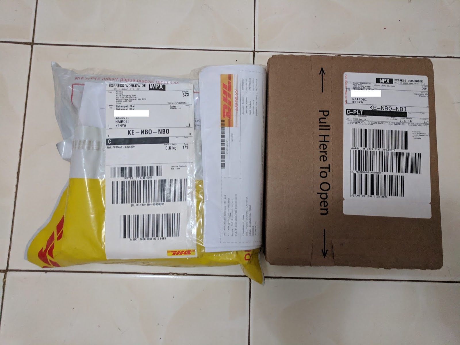
The harder part begins once the PCB design is done. Actually making this a physical reality in Kenya. I placed the usual order via PCBWay. A few days before Christmas before I went off to a round a country drive with some friends ( awesome content for another post). The shipping would be from Shenzhen via DHL. The logistics promises arrival by the 28th December.
Order Parts

The BOM for the design is not super complex either. Mouser covers the Kenya region. However there is no option for free DHL for orders over $60 which I get in Australia. I will be in Kenya only till the 20th January and the streets have no numbers or postcodes, which makes ordering via snail mail for any international shipping simply not fit the address template most places have. Perhaps global addressing via plus codes will become reality in future eCommerce systems. Mouser shipped the parts out of Texas immediately, I ended up paying more on shipping than for parts. The customs magic was yet to come.

Clear customs

Any packages with value below $1000 sail through customs in Australia. The Kenyan government will lose out on significant revenues if they followed this practice. On the flipside young engineers with limited resources are being stifled in self-driven learning and experimentation by this practice. I got a detailed/itemized bill from customs via DHL which ended up being the same cost as PCB + shipping for PCB's and around 20% of the cost of the parts. See file here for details and breakdown.


Source tools and materials

Thankfully this bit was much easier with a couple of local soldering iron , jumper wire and tweezers suppliers filling the gap. The ball was dropped by Fargo in delivering the stuff I ordered online again due to the addressing snafu, they attempted 5 deliveries to the wrong place before I had to redirect to the office address where a lot of parcels are received. I can recommend Nerokas and Ktechnics for getting parts in without hassle. Again better last mile logistics would have made things faster. I ended up attending the assembly meetup without the proper tools.

Find assembly space

To avoid annoying my landlord with solder fumes and messy paste workbench I started looking for a place to get together with a few interested parties and assemble the boards (at least one). I ended up starting an open-source hardware meetup and getting some Mang'u engineers together to hand solder the parts. 


Test and publish drivers


Finally this Sunday I have put together some basic micropython code to read registers from the CS5490 over serial and display them in a micropython notebook. Nothing production ready but proof that the PCB design and assembly worked as expected and we can achieve custom products here, with a lot of bureaucracy and false starts.

I am happy to meet more people designing and building open-source hardware in Nairobi and hear about their experience.