Showing posts with label teardown. Show all posts

Wednesday, June 26, 2019

Sunbeam Coffee Maker Teardown

The bad Kenyan grid has struck again. There is very little built in surge protection in the system, so all appliances plugged to the wall end up with in-house surge protectors. This time the victim was my beloved coffee machine which had served us well for more than a year.

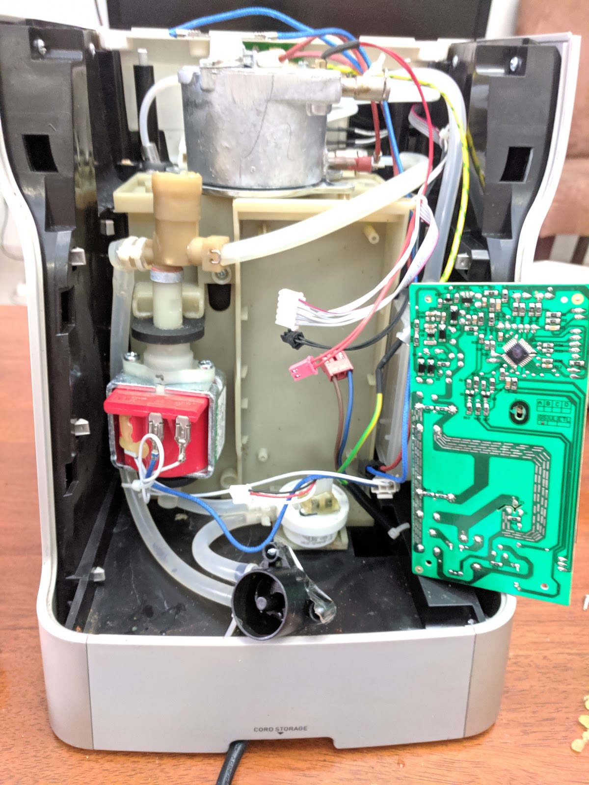
So I decided to take it home and spend some quality time with Pascal tearing it down. He is always curious about stuff and what is inside, so the Coffee machine is a complex beast capable of keeping him and myself occupied for hours on end. First we took of the top and looked at the heater and the electromechanical assembly controlling the hot-water head and frother was exposed. Also was exposed the heating tank with dual heating elements and a thermistor (I am assuming a thermistor rather than a thermocouple).

When we took the back plate off we found the main controller board. There is to obvious transformer in the set-up so I assume to whole power supply is cap-drop. There is a giant heat-sink attached to a 3-pin device which I assume is a triac or SCR for controlling the heating elements.

The bottom-left corner has a water pump with its own switching mechanism driven by relatively thin signal-wires from the main board.

There are some more interesting details on the main processor board including thick high current traces driven by the silicon switch with exposed copper and extra solder on top to increase thickness and provide a lower current path.

The main CPU is TQFP packaged micro-controller which is covered by the conformal coating the entire PCB is covered in. A macro image on twitter helped establish the lineage of the processor. It is a chinese 8051 variant with the datasheet here. Any help in translating it will be highly appreciated. But most of the schematic is legible.
Next up will be powering on the processor with a suitable 3.3v supply and examining the analog and digital buses. As well as powering on the whole thing to see why it turns of immediately on start. If the machine is unfixable I am planning to scavenge the thermistors, heating elements etc. to build a reflow mechanism.

All the water circulation mechanism is really interesting as well and can possibly be shoe-horned into a water cooler for a 3D printing system.

Sunday, March 3, 2019

Kogan Energy Monitor Teardown - Sonoff-Pow in a wall plug

After doing a tear-down on the TPLink Wall Plug energy monitor I found mentions in Australia of the much cheaper Kogan Alternative. So I decided to get a couple of them see what makes them tick as well.
General Assembly of the whole unit

TL;DR - The Kogan one is cheaper because it uses a bare metal (non-linux capable) CPU and a PWM output type energy monitor (without intricacies of a SPI protocol and calibration). It is essentially a repackaged Sonoff Pow.

The details of the build are packages in sections as I discovered them.

LV and Buck converter


The LV section consists of two separate cricuits:
  1. Relay to switch the load
  2. Buck converter to rectify and convert 240v to 5v to power electronics
The diagram below presents both of these sections. The Buck converter is basically the toplogy found in many aliexpress products. Perhaps with the difference of being unisolated (notice no slots). The relay is rated at 15A which is nice compared the TPLink product which uses x2 - 5A relays in parallel to achieve 10A.

Low Voltage (240v) Circuitry

Energy Monitor and LDO

This a 3.3v operated section which uses the super low-cost PWM output energy monitor IC made popular by the Sonoff the measure instantaneous voltage, current and hence power. The pulses are channeled to the main processor for forwarding to whatever backend Kogan has put together.

Metering and LDO

Main Processor

The design seems to have taken a standard ESP module and planted it on a basic PCB to fit in the power-plug form factor, sideways. The carries board has lots of markings and test-points making the task of reverse engineering and putting new firmware on this board almost too easy.
Processor module adapter
Marked bottom test pads of processor carrier PCB
Over all this looks like a nice certified unit which you can run your own firmware on thanks with the help of the right triangular security bit.

Sunday, November 18, 2018

TPLink Smart Plug Teardown

A while ago I remember watching a youtube video from about x10 years ago talking about distributed social network platforms running on SheevaPlugs. Fast forward 10 years, we are still in walled gardens of internet behemoths like Facebook, Twitter and Google and energy monitors are running full-linux os'es in smart plugs (albeit it is mostly OpenWRT/Lede)

The idea of re-purposing Atheros/Qualcomm router IC's as general purpose linux based controllers is not new. All those pins dedicated for ethernet ports are converted into GPIO's with proper muxing.

I have been designing one myself to fit in the DIN rail using the Onion Omega 2 as the host processor. There are some road-blocks regarding the simplex SPI bus on the Mediatek CPU.

TPLink seems to have gone the same route and built a smart-plug with and Atheros CPU. Again this blog post is meant to enrich the notes I already brain dumped on twitter.


This module is designed to be a wifi controlled relay with metering, switching upto 10A according to specs. It achieves this by using x2 5A relays in parallel. The main subsystems are:


  1. Power - Analog Devices/Linear Tech power AC-DC power IC. The footprint of this is an interesting variant of SOIC-8.
  2. Metering - This is done by the Maxim MAX71020A IC. Every electronics manufacturer worth its salt is creating metering ASIC's these days and I am excited about opportunities in making break-out boards and comparisons. TPLink seems to have bought up all the inventory of this particular Maxim IC and Maxim has a history of discontinuing low-margin lines the like MEMS accelerometers. I will keep an eye of the Poly-phase version which seems to be still in production (MAXQ3180). Overall this does not look good for the future of this particular smart-plug.
  3. Relays - x2 chunky 5v - 5A relays adorn the metering and CPU board. These provide the main functionality of the smart plug.
  4. Atheros/Qualcomm processor - This is the smarts in this smart-plug. Running standard open-wrt. The Maxim IC is of course on the SPI bus and other GPIO's are driving LED's , relays etc.
Overall the lack of supply of the Maxim IC does not bode well for the future of this Smart-plug. It may find fun alternative uses as an always on linux node.

Another Energy Monitor - Neur.io Teardown

Looking at other energy-monitor designs has been a past-time of mine and I recently the chance to teardown a Neur.io energy monitor installed along with many Tesla power-walls in Australia. This one had had some feedback of high voltage over the modbus and had fried itself. Despite best intentions with TVS suppressors etc. it could not take it anymore.

In this blog post I will enrich some of the content I already posted on twitter with some more in-sights in energy monitoring and additional elements regarding current clamps.

 This is the proper blogpost alluded to in the twitter thread. All the image content is already in the thread. Blogs simply allow greater structure. The meter is essentially composed of:


  1. Current samplers with 1ohm burden resisors attached to CT's - Neur.io recently announced a flexible CT design which can make it easy to install and potentially universal in measuring AC currents via induction and DC currents via hall-effect. I dropped an multi-meter probe on the burden resistors just to check.
  2. Voltage samplers as tiny encapsulated isolation transformers - This approach can introduce some non-linearity due to hysteresis and phase-shifts in the transformer, transformers are also bulky. Since the transformer is under no-load, phase-shifts should be minimal. The advantage is built in LV isolation. There is a bank of x3 transformers to account for x3 phases.
  3. Energy monitor IC's - These are from Cirrus Logic (CS5467), the documentation says the IC is mainly for the Japanese market. Neur.io seems to be successfully using it in North American and Australian market.
  4. Main processor and wifi - Unfortunately the unit I had was going back to Tesla under RMA, so I did not have chance to take of the shield and probe the processor. However I would love some assistance in poking in there and exploring the possibilities of custom firmwares.
  5. Modbus - The meter has a modbus I/O port to communicate with other systems e.g. Inverter and Battery charge controller.
  6. Power Systems - This is a Recom SMPS (RAC05-02SC) module keeping with my idea of keeping custom subsystems as limited as possible and reusing tested components as much as possible. I have seen a lot of energy monitors include their own power sub-systems including the Sense and WattWatchers. This increases design complexity with perhaps marginal improvements in design flexibility and BOM costs. The module outputs 3W at 5V, giving some head-room for LDO/Cap based noise filtering.
I have come to learn that DIN rails are not that popular in the North American market compared to the European and Australian market. Hence the overall brick packaging of the Sense and the Neur.io meters. Keeping the DIN form-factor requires a lot of combined mechanical and electronics design work as I have found out the hard-way. It is currently in my pipeline to create break-out boards for the CS5467 and test them out with common micro-controllers.

Thursday, December 14, 2017

Sense Energy monitor teardown - sampling in MHz

Recently I obtained a Sense Energy monitor via US from Margaret of BitKnitting. She is doing a very interesting neighbourhood energy efficiency project. As usual I could not contain my curiosity and opened it up to have a look. I will start off with an analogy - the closest bit of open-source kit that I have to do half the amount of analog functions as the Sense is the PRUDAQ on the BeagleBone wifi as pictured below.
Beaglebone Wireless + PRUDAQ
The case is very well built from high density plastic, however it is clipped together neatly and easy to take off without permanent damage. The wifi antenna is screwed on with a neat water sealed connector. The power/voltage and current sampler connectors are Molex Microfit and Nanofit respectively. I rather liked the Molex Nanofit and adopted it for my own DIN Rail sampler board.
Enclosure and main boards
Inside this very nice exterior are a couple of very dense sandwiched PCB's. One is Green, almost a generic power supply board, but with additional function to sample the split phase AC in the North American grid. The other is a black board where the magic happens. It is essentially a beaglebone wireless with a custom energy monitor system put together using high-speed ADC's and a CPLD
Green Power board, Black Digital+Analog board

Main PMIC, same one is used on the BeagleBone Black
The image below shows the subsection that performs energy measurements, it is composed of x2 high sample rate ADC's (14bit 2MSPS) and an Altera Max V 64pin CPLD. I assume the cells inside the CPLD perform the reading from the ADC's and multiplication/accumulation to compute energy usage, then transmit computation results to the TI CPU.

Custom energy monitor with high-speed (2MSPS) ADC's and Altera CPLD

Wifi Module
Switcher IC's on power supply board

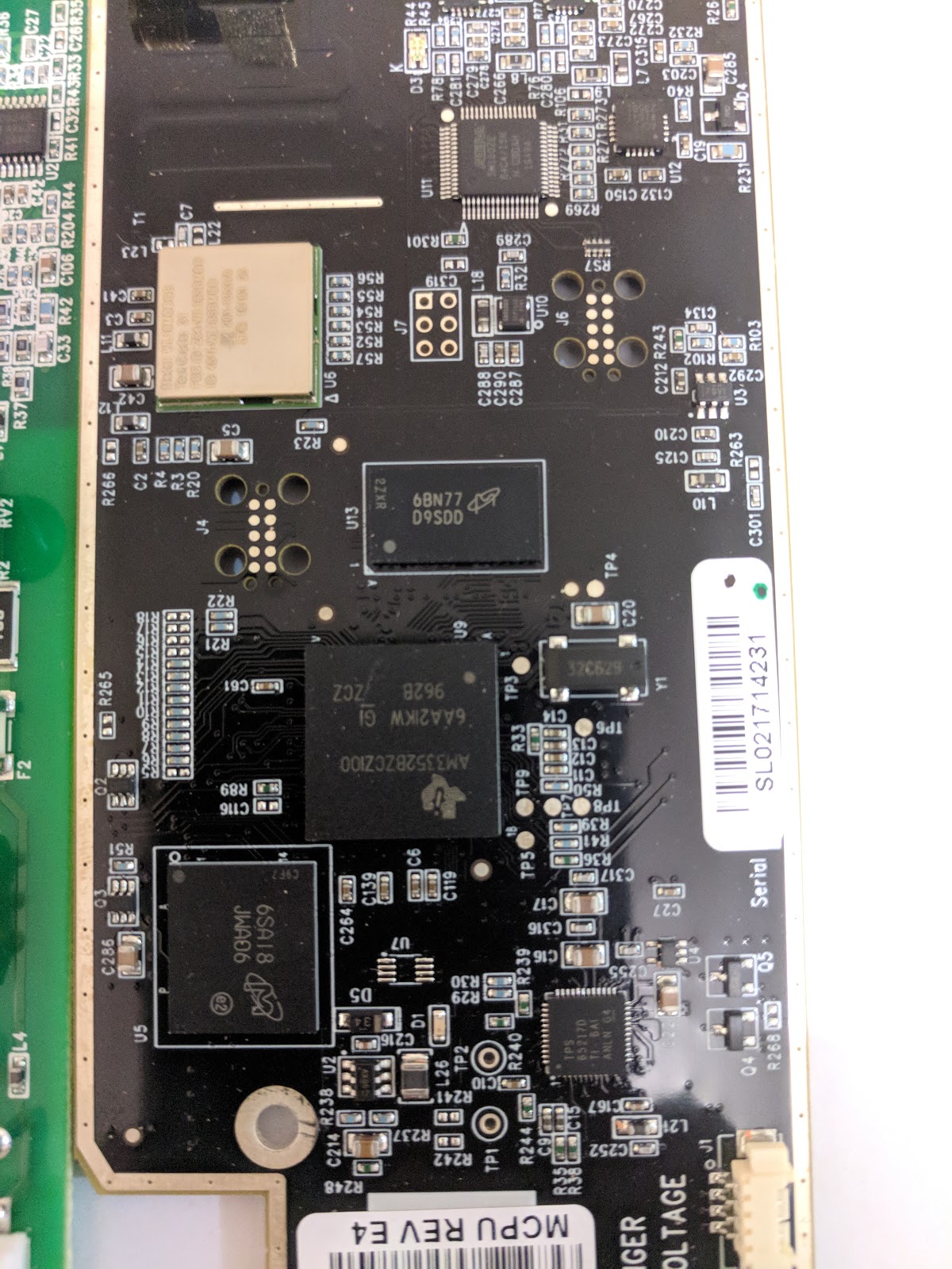
The main CPU is a Linux compatible AM3352 CPU from TI. It does not have a PRU co-processor like the one used on the BeagleBone, hence the need for a CPLD to perform some of the real-time computation required.
TI Arm CPU and RAM/Flash

Overall the Sense energy monitor hardware is a great design, though a bit specific to the USA market. I am looking forward to a release in the Australian market. The purchase to study one was certainly worth it. Now off to install my own linux build on it and send the data elsewhere.

Thursday, June 29, 2017

3G Energy Monitor - WattWatchers teardown

Tear-downs are always done in a spirit of learning and admiration. Having built some hobby electronics I really appreciate what goes into laying out a mixed signal PCB as well as one that has high and low-voltages on the same board and is subject to regulatory compliance both for electrical characteristics and RF emissions.

I was handed some detailed WattWatchers images by a client and I did some mark-up of what goes into them based on previous experience of how energy monitors are put together. It is a 2-board design with an SMD PCI connector joining the boards. The PCI connector passes the power and current-voltage signal up to a vertical board.

I shall call the bottom board power and sampling  board and the side-board metering, CPU and network board. The first image below shows one side of both boards. The power supply board features a hefty cap-drop supply with assortment of fuses and TVS, as well as the aforementioned PCI connector. The vertical board features a large 3G module and associated Telstra sim slot, I assume the SIM is linked to a custom M2M plan which costs a few dollars a month.

The other side of the vertical board features the most interesting goodies. On the left half it has a low-noise / high power voltage regulator from ST (presumably needed to feed the hungry 3G modules), as well as a low-power MSP430 MCU with a couple of large old-school tantalum caps. The right side of this board (separated by a row of what is most likely transient suppressors or isolation amplifiers) are a couple of Analog devices 3-phase energy monitor IC's. The isolation section indicates the presence of 9 analog channels which corresponds to 3-phases and 6-CT's. The 2 ADE7880's share a single clock crystal presumably buffered. There are also a bunch of passives to perform 50Hz filtering.

The other side of the bottom board also featured in this image contains the voltage divider to sample the AC-phases and some current-multiplier/burden resistors to convert the current measured by the CT's into a voltage value. There is also another LDO on this board to presumably power one side of the isolation amplifiers, nothing too high power. This LDO must be at the end of the cap-drop system so the neutral or phase on it is at high voltage and generous dob of insulating snot is providing extra protection. The insulating snot can also be seen at the top-left corner of this board where the phase and neutral(?) or 2 phases are too close together for comfort/compliance.

WattWatchers has done a great job packing a lot of features into an M2 DIN rail enclosure without resorting to many off the shelf modules and pre-built components except the 3G module. I am hoping to re-use some of the concepts here in my ATM90E36 based design.

Wednesday, December 7, 2016

Aliexpress DIN Rail Energy Meter teardown

The best way to learn is often by looking at solutions others have come up with. "Monkey see - monkey do" is pretty much part of the engineering process. While at University we wrote a top-scoring piece on how Apple scooped Creative in making a portable digital hard drive backed music player with great design and even greater marketing. When doing a tear down for inspiration and copying ideas always be wary of patents.

I am planning to move my ATM90E26 + Wireless Stack Energy monitor into a more industrial DIN rail format. To get an idea about how things are packaged inside a DIN rail energy monitor I ordered a no-patents cheap energy monitor with pulse output from AliExpress. The brand is Eastron, they also make quite affordable 3-phase versions which I am going to look at next.
DIN rail enclosure including wiring diagram
Once the meter arrived I did not even plug it in (in Australia an electrician will be required to properly install it due to the cutting of the live line to place a shunt and other modifications). I put a screw driver through the QC sticker, popped open the clipped on enclosure and proceeded to have a peek inside. What I found was a house of PCB's stacked around a transformer to make best use of the place inside the enclosure. The following labelled photos show the various parts.
Profile view with stacking

The stacking places the main processor board with AFE + MCU and LCD display on top, the transformer and associated carrier and high voltage safety stuff (Varistor and PPTC) at the base. The base PCB also carries the Live/Neutral connectors and a bulky current shunt. One vertical PCB is the power supply, voltage and current waveform sampler and the other is an isolated pulse and modbus output board (Modbus chip is unpopulated in my pulse only version).
Bottom view with safety components and current shunt
The voltage sampler uses a resistor ladder of 4x270K resistors in series with a relatively small voltage sampling resistor. The PCB is not heavy on expensive board to board connectors, which allows a modular system and swapping of boards, instead it relies of solder fingers on board edge to link the boxy shape together. The same board also carries the power supply module derived from a regulated full wave rectified output from the transformer. I am not sure if the transformer is isolating, it does not need to be since the isolation occurs at the end stage with a couple of optocouplers. The voltage sampler and the current shunt are obviously non-isolated.
LDO for dual voltage level output and 4 pads for 2 waveform signals
All the magic of actual energy monitoring then happens in the Vangotech V9811S with includes a 8052 MCU for driving the LCD and other functions such as Modbus support. I am planning to power it up with a 3.3V/5V supply and feed it waveforms from my low voltage AC test rig and observe the readings. I also have 3 phase version from Eastron on order and a few engineering samples from Vangotech for their 3 phase ASIC to build a low cost/ low voltage Dev kit like I did with the ATM90E26 Featherwing.
Anatomy of the head, MCU + AFE, EEPROM and an old school LCD